Japan Interlocking Boxes Market Advances Circular Packaging with High-Strength Paper Material Innovations
Other |
2026-07-14 07:15:08

Upgrade auf Pro
The frontier of nanotechnology is currently defined by the ability of scientists to manipulate matter at the molecular level, a task that relies heavily on the advancement of polymer science. Modern research is focused on developing "Directed Self-Assembly" (DSA) techniques, where the photoresist itself is engineered to form specific patterns through chemical thermodynamics rather than just light exposure. This hybrid approach promises to push resolution limits beyond what is traditionally possible with optical lithography. Current Photoresist Market Research highlights the importance of these collaborative academic and industrial efforts in overcoming the "stochastic" effects that cause line-edge roughness in sub-7nm nodes. By improving the molecular weight distribution and the uniformity of the polymers, researchers are aiming to create a smoother, more reliable canvas for the world's most complex circuits.
Beyond the polymers, the solvents and additives used in these formulations are also undergoing significant scrutiny. Researchers are looking for greener alternatives to traditional solvents that do not compromise the performance or safety of the cleanroom environment. This involves testing new organic compounds that can offer the same solubility profiles while being more biodegradable. Additionally, the development of "dry" resist technology—where the material is deposited via vapor rather than liquid spin-coating—is a burgeoning area of study. This could potentially eliminate many of the defects associated with liquid application and drying. As these scientific breakthroughs move from the lab to the production floor, they will redefine the standard operating procedures for fabs globally, ensuring that the limits of miniaturization are continuously challenged and surpassed.
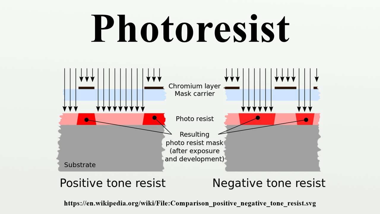
What is "Line-Edge Roughness" (LER) and why is it a problem? LER refers to the microscopic irregularities along the edges of a printed line. At extremely small scales, these bumps can lead to electrical leakage or performance inconsistencies, making it a major focus of current research.
How does "Spin-Coating" work? It is a process where a liquid photoresist is dropped onto a spinning wafer. Centrifugal force spreads the liquid into an incredibly thin, uniform layer across the entire surface, which is critical for consistent patterning.
➤➤➤Explore WiseGuy’s Related Ongoing Coverage In Semiconductor Industry:
Temperature Transmitter Market
Thermal Drone Inspection Market
Thermography Condition Monitoring Equipment Market
Thin Film Deposition Equipment Market