English
 Arabic
 French
 Spanish
 Portuguese
 Deutsch
 Turkish
 Dutch
Dutch
 Italiano
 Russian
 Romaian
 Portuguese (Brazil)
 Greek
Greek
A Homeowner's Guide to Catching Sewer Line Problems Before They Cost You
Home |
2026-08-13 10:45:30
 Advertise With Us
 About Us
 Terms And Conditions
 Πολιτική Ιδιωτικότητας
δες τα όλα
Πολιτική Ιδιωτικότητας
δες τα όλα

Upgrade to Pro
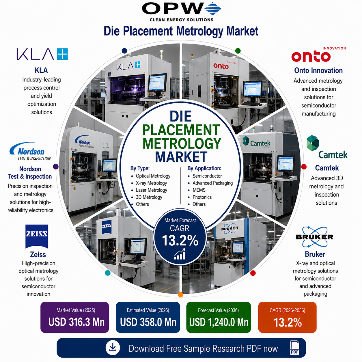
According to a comprehensive market research report published by Fact.MR, The global Die Placement Metrology Market crossed a valuation of $316.3 million in 2025 and is projected to increase from $358.0 million in 2026 to $1.24 billion by 2036, recording a compound annual growth rate (CAGR) of 13.2% over the forecast period.
Get detailed market forecasts, competitive benchmarking, and pricing trends: https://www.factmr.com/connectus/sample?flag=S&rep_id=15657
This expansion represents an absolute dollar opportunity of $882.0 million over the ten-year period. Rapid market adoption is being driven by outsourced assembly and test (OSAT) providers and foundries scaling 2.5D interposer and 3D stacked die architectures, where isolating die placement drift from substrate distortion and thermal expansion is critical to maintaining interconnect yields.
Key Die Placement Metrology Market Highlights at a Glance
Why Is the Die Placement Metrology Market Growing?
Demand for die placement metrology systems is accelerating as semiconductor packaging migrates toward ultra-fine interconnect pitches and multi-chiplet modules. Three key process imperatives are driving capital equipment adoption:
"Placement metrology is shifting from a final quality audit toward active in-line feedback that corrects the next placement in real time," states Ganesh Pai, Lead Semiconductor Analyst at Fact.MR. "As multi-chiplet 2.5D interposers and 3D stacked dies shrink interconnect pitch, separating mechanical stage drift from thermal expansion and substrate distortion becomes essential to preserving high-volume manufacturing yield."
How Does the Market Break Down Across Major Segmentation Axes?
Package Type: Why 2.5D Interposer Packages Lead Demand
2.5D interposer packages are projected to represent the leading package segment, holding a 47.2% market share in 2026. Integrating multiple heterogeneous dies across a large silicon or glass interposer requires high-speed spatial registration to guarantee alignment across all chiplet interfaces.
Measurement Stage: Why Post-Placement Metrology Dominates
Post-placement measurement is forecast to hold a commanding 41.5% market share in 2026. Measuring die position immediately following placement isolates placement error before thermal compression, reflow, or adhesive curing forces introduce secondary positional movement.
Metrology Technique: Why Optical Microscopy Metrology Leads
Optical microscopy metrology is projected to hold a 30.0% share of the metrology technique segment in 2026. Optical systems provide non-contact, rapid measurement of alignment fiducials across wide fields of view without impeding production throughput.
Accuracy Class & End User: Sub-0.5 µm Accuracy and OSAT Adoption
The sub-0.5 micrometer (<0.5 µm) accuracy class is forecast to capture 40.2% of the market in 2026, while OSAT providers represent the leading end-user segment with a 29.5% market share. OSAT houses require reconfigurable, ultra-high-precision metrology platforms capable of processing diverse customer packaging formats.
Die Placement Metrology Market Dynamics
Market Drivers
The primary market driver is the proliferation of high-density heterogeneous integration architectures. As chipmakers combine logic, memory, and optical chiplets on single substrates, automated placement metrology is required to decompose multi-factor placement errors and eliminate yield losses.
Market Restraints
The key market restraint involves optical access and throughput bottlenecks. Sub-micron optical measurement can restrict assembly line speed when field of view, illumination angles, and calibration routines are not directly integrated into the high-speed bonder cell.
Key Market Trends
A major market trend is the integration of real-time thermal drift compensation models during thermal compression bonding (TCB). Fabs are deploying closed-loop metrology frameworks that feed alignment data back into bonder controllers to dynamically offset thermal expansion errors.
Regional and Country Outlook
Capital spending on die placement metrology equipment is heavily weighted toward Asia-Pacific packaging hubs due to concentrated OSAT manufacturing capacity and foundry expansions.
Taiwan is projected to be the fastest-growing national market globally, expanding at a 14.8% CAGR through 2036. Growth is fueled by continuous capital investment from leading foundries, advanced packaging facilities, and a dense ecosystem of substrate suppliers.
Malaysia follows with a projected 14.0% CAGR, supported by its status as a major global center for outsourced assembly, test, and packaging operations.
The United States, China, and South Korea continue to demonstrate strong equipment demand as domestic semiconductor initiatives accelerate advanced chiplet manufacturing and memory packaging capacity.
Competitive Landscape
The competitive landscape in die placement metrology includes specialized optical inspection providers and broad-line semiconductor metrology suppliers.
Equipment vendors are increasingly differentiating through software intelligence, delivering automated error-decomposition algorithms and closed-loop communication protocols that connect metrology systems directly to die bonder stages.
Read the Comprehensive Industry Report: https://www.factmr.com/report/die-placement-metrology-market
Frequently Asked Questions
What is the projected market size of the Die Placement Metrology Market by 2036?
The global Die Placement Metrology Market is projected to reach a valuation of $1.24 billion ($1,240.0 million) by 2036.
What is the forecast growth rate (CAGR) for the Die Placement Metrology Market?
The Die Placement Metrology Market is expected to expand at a compound annual growth rate (CAGR) of 13.2% between 2026 and 2036.
Which package type segment commands the largest share of the market?
2.5D interposer packages represent the leading package segment, holding a 47.2% market share in 2026.
What is the dominant measurement stage in the die placement metrology market?
Post-placement measurement is the leading measurement stage, capturing a 41.5% market share in 2026.
Which metrology technique holds the largest market share?
Optical microscopy metrology is the leading technique segment, accounting for a 30.0% market share in 2026.
Which country is expected to exhibit the fastest growth rate in this market?
Taiwan is forecast to be the fastest-growing national market, expanding at a 14.8% CAGR from 2026 to 2036.
Who are the leading equipment manufacturers operating in the Die Placement Metrology Market?
Key companies operating in the market include KLA Corporation, Onto Innovation, Camtek Ltd., Bruker Corporation, Nordson Test & Inspection, and Carl Zeiss AG.
To View Related Report:
Dielectric Material Market: https://www.factmr.com/report/dielectric-material-market
Audience Intelligence Platform Market: https://www.factmr.com/report/audience-intelligence-platform-market
Embodied AI Safety Certification Services Market: https://www.factmr.com/report/embodied-ai-safety-certification-services-market
Ingredient Discovery Platform Market: https://www.factmr.com/report/ingredient-discovery-platform-market
To View More Report:
Chiplet Surface Cleaners Market: https://www.openpr.com/news/4584996/u-s-chiplet-surface-cleaners-market-basf-strengthens
Fluxless Attach Systems Market: https://www.openpr.com/news/4585023/u-s-fluxless-attach-systems-market-indium-corporation